@RobGrieves
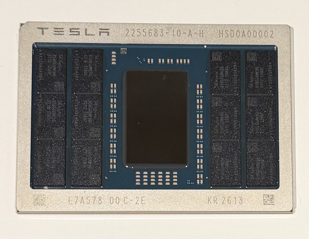
Let's talk about the AI5 picture. Memory From what I can gather from the grainy low res photo, those RAM chips appear to be SK Hynix H58G66DK9QX170N 8GB LPDDR5X with 9600Mbps bandwidth. 12 modules = 96GB @ 1.15TB/s The Die Size appears to be half-reticle (~430mm2). This gives it a yield and cost advantage over full reticle dies such as Nvidia's H100 (<800mm2). If we assume Tesla is using TSMC 3nm process, this gives the chip 108-125B transistors. Performance With that many transistors and memory performance, when constrained to ~150W such as a car or Optimus, we're looking at 2000-2500 TOPS which matches up nicely with a H100. Unconstrained, such as in a datacentre it could be much more. The Package This packaging is pretty cool. It includes memory on package which gives huge memory latency advantages than the typical memory on board config. To me, this amount of RAM packaged in this way is way overkill for a car. I believe we're looking at the datacentre version in this image. I believe for the cars or Optimus, we will see a traditional memory on board config (with less of it - e.g 32GB).